Photonics, which operate based on particles of light (photons), are increasingly important for applications such as optical communications, connections between electronic and optical networks, and imaging. But silicon, the go-to semiconductor for making electronic chips, is not a great material for photonic applications because it shows poor absorption of near-infrared light compared to other semiconductors such as gallium arsenide. On the other hand, gallium arsenide is difficult to integrate with silicon microelectronics. As a result, photonic devices are expensive to manufacture.
Now, Professor Saif Islam and colleagues at the UC Davis Department of Electrical and Computer Engineering have come up with an approach that dramatically increases the photon absorption of silicon. The work was published July 24 in Advanced Photonics Nexus.
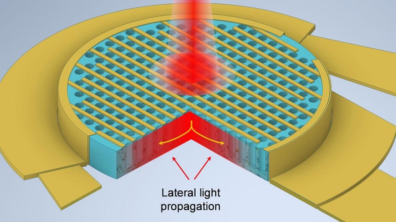
They created a micrometer-thick wafer of silicon with regular tiny holes in it. When infrared light hits the wafer, it is "trapped" by these structures, bends almost 90 degrees and travels sideways through the wafer, increasing contact with the semiconductor and absorption of photons.
Simulations by the team showed that this photon trapping increases absorption by several times over a plain silicon wafer and actually outperforms gallium arsenide.
Because the approach is compatible with chip manufacturing technology, it could enable a new generation of cheaper photoelectronic devices.
